2/17 SANYANG MOTOR
筑波醫電
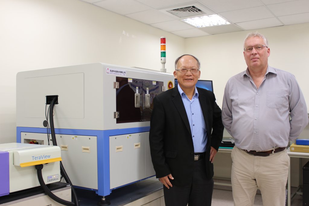
Hsinchu, Taiwan – ACE Solution, the leader and the provider in customized test solutions to meet customer needs in electrical components, devices and system manufactures, is pleased to announce the product launch of the TZ6000 – a nondestructive wafer quality measurement tool for the compound semiconductor industry. Incorporated with TeraView’s TeraPulse Lx technologies, the TZ6000 achieves nondestructive wafer quality measurements of thickness, refractive index, resistivity, dielectric constant, surface/subsurface defects at selected positions and whole wafer scanning map.
Dr. JC Chen, VP of R&D of ACE Solution, commented “The quality of the semiconductor wafer determines the maximum achievable conversion efficiency to the final device. Subsurface damages (SSD) of semiconductor wafers are easily induced during surface machining process includes rough grinding, fine grinding, and chemical mechanical polishing. Current wafer inspection systems which rely on VIS/IR/UV optical inspection can analysis the surface properties of the wafer but not the SSD, due to their low penetration depth. Terahertz (THz) wave has higher penetration depth in semiconductor wafers as silicon, silicon carbide and gallium nitride. We developed the THz-based TZ6000 to meet the market need of nondestructive inspection of the compound semiconductor wafer.”
Dr. Philip F. Taday, Head of Applications and Principal Scientist of TeraView, commented “The TeraPulse Lx system is TeraView’s world-leading product family for terahertz analysis. It has been designed to meet the needs of the material inspection in imaging or spectroscopy applications, and is ideal for compound semiconductors. The system’s modular architecture and TeraView patented laser-gated photoconductive emitters and detectors gives the user both flexibility and expandability. The system also boasts an industry-leading 3,200 ps time-delay line, as standard.”
Steve Hsu, CEO of ACE Solution, commented “ACE Solution is the leading company in providing electrical precision test, integrating service and solution. It is great opportunity to collaborate with TeraView and incorporate the TeraPulse Lx module into TZ6000 system for nondestructive wafer quality inspection. TZ6000 has high flexibilities for various sizes and forms of wafers. It is provided with TeraView’s unique THz-TDS probe for simultaneous measurement of multiple parameters of wafer characterization. TZ 6000 has a user-friendly and graphic illustrate software for quality inspection in wafer manufacturing process and R&D.”
Dr. Don Arnone,CEO of TeraView, commented “This is another first from TeraView to have a close collaboration with ACE Solution to develop this product, and we are quite confident that this product will set a new standard in compound semiconductor wafer quality analysis and defect inspection. The TeraPulse Lx system is designed with a lightweight compact core unit which allows for easy transport between locations. Incorporated with TeraView’s TeraPulse Lx modules, we can address the growing needs of the compound semiconductor wafer industry with this product.”
About ACE Solution
Founded in 2000, ACE Solution (https://www.acesolution.com.tw/en/index/) is located in Hsinchu City, Taiwan with branch offices in Suzhou and Shenzhen in China. Our mission is to provide customized test solutions to meet customer needs in electrical components, devices and system manufactures, as well as providing technology solutions through our partners. We are focused on RF, mmWave and terahertz with the expert technical support team. ACE Solution provides professional, innovative and multi-functional integrated techniques and solutions.
About TeraView
Founded in 2001, TeraView (https://teraview.com/) is the world’s first and leading company solely focused on the application of terahertz light to provide solutions to customer issues. A spin out from the Toshiba Corporation and Cambridge University, TeraView has developed its proprietary technology across a number of markets. These include fault analysis and quality assurance for semiconductor chips used in mobile computing and communications, as well as non-destructive inspection of high value coatings used in the automotive, pharmaceutical, food and solar industries.
Contact
ACE Solution, Co., Ltd.
Address: 2F-1, No.28, Taiyuan street, Jhubei City, Hsinchu County, 302, Taiwan
Telephone: +886 3 5500909
E-mail: thzlab@acebiotek.com
WebSite: https://www.acesolution.com.tw/en/index/
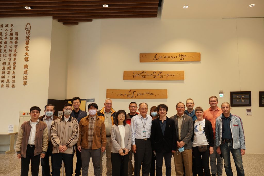
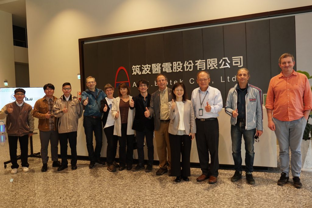
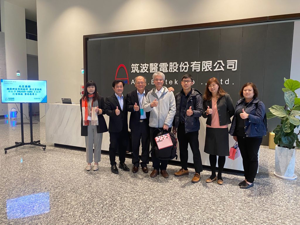
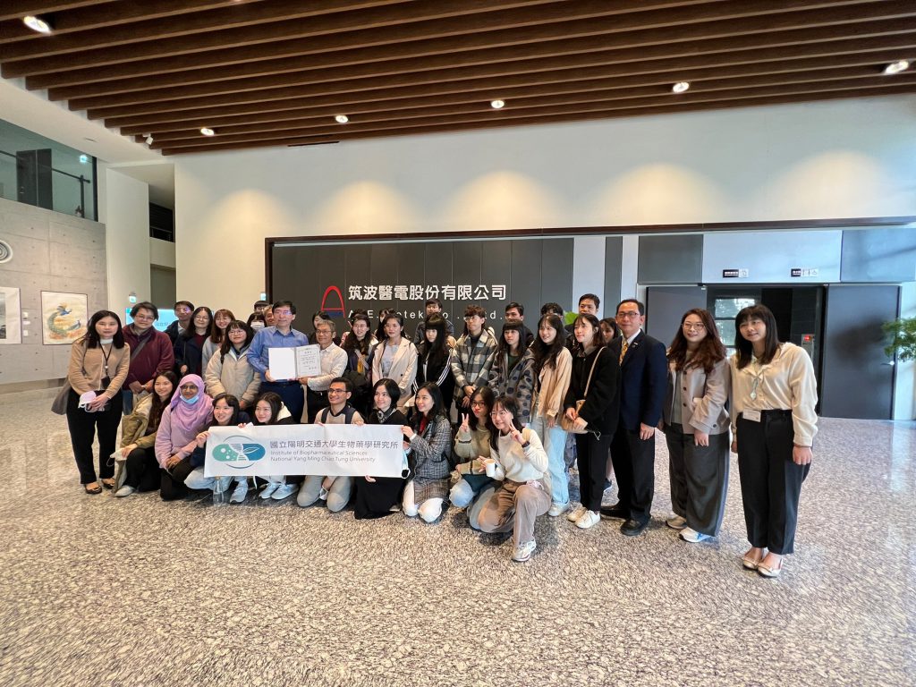
ACE Group develops smart hospital upload systems and third-generation semiconductor material testing solutions based on 20 years of wireless communication, IoT, software, and hardware integration experience. National Yang-Ming Chiao Tung University (NYCU) and Linköping University (LiU) visit the enterprise to see digital healthcare, Terahertz (THz), and semiconductor performance.
Industry-Academy Platform to Build Compound Semiconductor Advanced Materials Cooperation
NYCU conducts a crucial project on the compound semiconductor. It applies advanced materials such as silicon carbide (SiC), gallium nitride (GaN) and gallium oxide (Ga2O3) to Power IC and RF. The project can build up advanced materials, software services, and platform design. Moreover, this can reach industry-academy partnerships. The Thin Film Physics Division of LiU conducts application-inspired basic research on thin films to fundamentally understand the atomistic nature of materials’ properties and behavior and learn how to make materials perform better through new methods of synthesis and processing. The research concerns the design of new multifunctional materials for rigid and wear-resistant coatings, energy materials, magnetic materials, electronics, neutron-converting materials for the European spallation Source (ESS), wide-band gap semiconductors, and more.
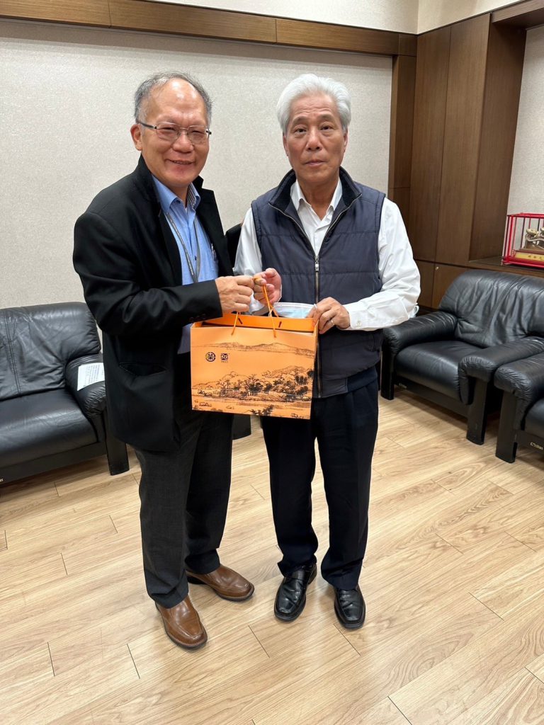
Prof. of NYCU, Horng, Ray-Hua recognizes that” ACE Group differentiates from other material testing companies. We look forward to cooperating with THz technology on non-destructive detection and failure analysis of materials; on the other hand, the Uniiform digital handwriting system can contribute to education.” The Professors from LiU also indicates that the THz technology is awe-inspiring and suggests that the possibilities with polarized waves, used for instance in THz-ellipsometry, may further improve and expand the technology. The visitors also commented that the Uniiform digital handwriting system could be a great tool in education.
ACE Group Competitive Advantages: Wireless Communication, Smart Hospital, and Semiconductor Integration Testing
ACE Group specializes in RF electronic components, measuring instruments, communication system tests, and integration. Since 2014, the company has been committed to digital medicare and precision medical treatment of early diagnosis technology and devices. Combined with AI, it invents the Uniiform digital handwriting system and Data Stream (DS) for Anesthesiology (Spark), Ophthalmology (Eagle Park 100), and Dentistry medical form digital recording system particularly. ACE uses THz technology (TZ-6000) for wafer testing in the semiconductor testing field. Nowadays, ACE establishes partnerships with Teradyne to promote Eagle Test System (ETS). For the third-generation semiconductor, ETS can fulfill the high voltage and high current test solutions in automotive semiconductor production test requirements.
ACE Group invites Dr. Philip F. Taday, the scientist of Teraview, to join the panel discussion at this event. Electro-Optical Terahertz Pulse Reflectometry (EOTPR) is an innovative time domain reflectometry (TDR) system that Intel and TeraView have successfully developed. It uses the isolation technique that is the first place in the world to detect package failures and monitor the quality of integrated circuits. It’s the first choice for non-destructive defect detection of integrated circuit packaging. Interdisciplinary skills swapping creates the novel industry application and research of advanced semiconductor materials.
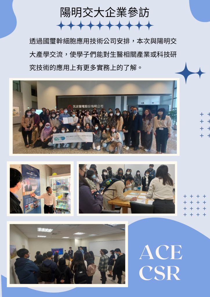
筑波集團從3C到3醫,基於20年無線通訊、IoT軟硬體整合經驗,開發智慧醫院上傳、第三代化合物半導體材料測試等方案。國立陽明交通大學及瑞典Linköping University (LiU)林雪平大學率團來訪交流,參觀智慧醫療、太赫茲(Terahertz, THz)應用及半導體方案應用成果。
產學跨界平台鏈結半導體創新材料應用
陽明交大承接國科會化合物半導體重大發展計畫之一,將碳化矽(SiC)、氮化鎵(GaN)與氧化鎵(Ga2O3)等新材料應用於Power IC、RF,藉此開發鏈結創新材料、軟體服務及設計平台成果,並透過跨產業與學術交流活動促成跨界合作。林雪平大學薄膜物理團隊(Thin Film Physics Division)對薄膜進行應用啟發的基礎研究,從根本上了解材料特性和鍍膜行為,並學習如何通過新的合成和加工方法使材料性能更好。研究涉及新型多功能材料的設計,用於硬質耐磨塗層、能源材料、磁性材料、電子產品、中子束繞射材料、寬帶隙半導體等。
陽明交大洪瑞華教授肯定:「筑波有別於其他材料檢測的公司,雙方能合作將THz技術用於非破壞性檢測、材料缺陷等分析,Uniiform智慧手寫輔助系統則對教學輔助非常有幫助」;林雪平大學的團隊表示:「筑波智慧手寫輔助系統及材料檢測技術令人印象深刻,若能加入光偏振的THz橢偏儀技術,將能更進一步提升檢測技術應用層級並更廣泛的被用於半導體晶圓測試市場」。
筑波集團三大即戰力:無線通訊、智慧醫院、半導體整合測試
筑波集團致力於無線通訊、RF量測儀器設備、高頻、電子元件/模組等整合測試方案。自2014年起投入智慧醫療領域致力於早期病變精準醫療之篩檢技術與設備研發,結合AI開發Uniiform、智慧上傳閘道器(Data Stream, DS),各科別整合上傳方案如Spark智慧麻醉紀錄系統、看得健100智慧眼科紀錄系統、牙科。在半導體測試領域,筑波的THz技術之TZ-6000用於半導體晶圓測試市場,並與美商泰瑞達Teradyne攜手推廣Eagle Test System (ETS)系列,針對第三代半導體高電壓、高電流之車用測試提供整合設計,滿足各產業鏈客戶需求。
本次交流亦邀請TeraView 的科學家Dr. Philip F. Taday共襄盛舉,Teraview的電光太赫茲脈衝反射儀(EOTPR) 是世界上第一款使用隔離技術來檢測積體電路中封裝故障和監測封裝品質,是廣用作為積體電路封裝非破壞性缺陷檢測首選。藉由跨領域的切磋開創先進半導體材料研究、業界創新應用。